More details will be available in August 2025
Thank you to our Keynote Speakers from SWTest Asia 2024!
Thursday Keynote Speaker

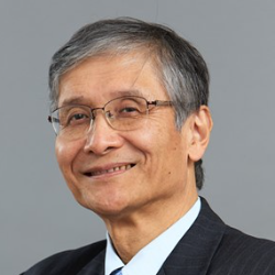
Hiroto YASUURA, PhD
National Institute of Information – Japan
Hiroto Yasuura is a Professor Emeritus of Kyushu University. He is also a Vice Director General (Chief Cyber Science Infrastructure Director) of National Institute of Informatics (NII). He also serves for Ministry of Education, Culture, Sports, Science and Technology (MEXT) and Japan Science and Technology Agency (JST) as chairs of several committees. Additionally, he has worked for several local governments as advisors and private companies as independent directors.
Prof. Yasuura received the B.E., M.E. and Ph.D. degrees in computer science from Kyoto University, Kyoto, Japan, in 1976, 1978, and 1983 respectively. He was an associate professor in Kyoto University and moved to Kyushu University in 1991 as a professor. In Kyushu University, he conducted research projects on the system LSI design methodology, which includes data-path width optimization, low-energy system design, SoC architecture and a core base LSI test method. He also promoted education of VLSI design in computer science area in Japan with VDEC (VLSI Design and Education Center) in University of Tokyo.
He served as the research director of Silicon-Sea-Belt Fukuoka from 2001, to build up a research-industry cluster on LSI design. More than 250 LSI design related companies moved to or were established in the Fukuoka area in the last 25 years. He is also one of the founders of ISIT (Institute of Systems, Information Technologies and Nanotechnologies, established in 1995), which is founded by Fukuoka city for promoting ICT industry.
He served as Technical Program Chair and General Chair of ICCAD in 1997 and 1998, respectively, Vice President of IEEE CAS Society, an ACM SIGDA advisory board member, General Chair of ASP-DAC 2003, and Steering Committee Chair of ASP-DAC. He is a fellow of IEEE, IEICE (Institute of Electronics, Information and Communication Engineers) and IPSJ (Information Processing Society of Japan).
Keynote Topic:
Silicon Seabelt 2.0: Challenges of Kyushu for Reproduction of Silicon Island
Kyushu was called Silicon Island in the 80’s and 90’s. With the opening of TSMC’s factory in Kumamoto, we started a new step of revitalization of the silicon island. Leveraging integration of over 1000 companies related with semiconductor industry, we are restoring the activities on education, industrial eco-system and business environment for modern semiconductor industry. By the collaboration with Taiwan, Korea and South-East Asian countries, we have launched the project Silicon SeaBelt 2.0.
The talk includes various activities and collaborations of Japanese central and local governments, universities in Kyushu area and industrial partners in Kyushu and foreign countries.
Friday Keynote Speaker

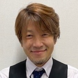
Shinya AKATA
Sony Corporation – Japan
Shinya Akata is a seasoned semiconductor professional with a strong background in test engineering and design for testability (DFT). Akata-san joined Sony Corporation in 1995 and has held various leadership roles, including Test Engineer, DFT Engineer and Test Leader. In 2019, he was dispatched to Sony Semiconductor Manufacturing Corporation to serve as the Senior General Manager of the CIS Test Engineering Division. Currently, he is the Deputy Senior General Manager of the Design & System Technological Platform Division at Sony Semiconductor Solutions Corporation.
Keynote Topic:
Critical Role of Test for Image Sensor Development
Image sensors have become an integral part of our modern world, powering devices from smartphones to autonomous vehicles. SONY, a pioneer in this field, has developed a global reputation for producing high-quality image sensors that deliver exceptional performance. As the person responsible for testing these critical components, I believe that a rigorous testing process is essential to ensure their reliability and functionality. In this presentation, we will discuss the critical processes that allow the next generation of devices to shine through their strengths and eliminate their weaknesses with thorough test strategies.
Friday Keynote Speaker

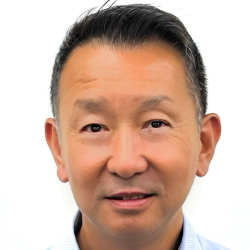
Tetsu Ozawa
Socionext Inc. – Japan
Tetsu Ozawa is the General Manager of the Production & Quality Management Group, Product Engineering Division, at Socionext Inc. Headquarters in Yokohama city, Kanagawa prefecture, Japan. His team is responsible for testing technologies and yield management for all products of Socionext.He has more than 30 years of experience in test development and test engineering and is currently responsible for test management (technologies, quality, costs, equipment, components, capabilities, delivery dates, resources). Since then, he has been involved in the outsourcing business for IDM company and fabless company for over 15 years, and now as fabless, he has win-win relationship with global eco-partners to run the outsourcing business. Socionext will continue to provide stable supply of leading-edge, high-quality SoC products to global customers through superior testing technology.
Keynote Topic:
New Wafer Testing Challenges for Leading-Edge SoC Products
Socionext has built a new business model “Solution SoC” to provide SoC products to global customers seeking leading-edge and innovative chips. Socionext is focusing business on the advanced custom chips in the automotive, data center/networking and smart device markets. At present, in the leading-edge semiconductor market, with the evolution of the advanced wafer process node, enlargement of the device, increasing high-current, and high-speed rapid advance are crucial. In addition, leading-edge chips and packaging technologies are constantly developing, further increasing the value added to chips and assemblies.
We believe that the expectation and importance of advanced testing technology are more profound than ever, and that we are in a period of great change. We also believe that the establishment of new testing technologies and the linkage of new semiconductor value chains will bring significant benefits, such as improved yield and quality. In addition, it is necessary for us to adapt to flexible semiconductor process flows to make profits in various advanced products in the future. Therefore, we are promoting the establishment of a technology to change the test in real time according to the manufacturing situation and to shift the process flow to the left or right. Among these activities, wafer testing is very significant.
In this article we will introduce the development status of Socionext’s leading-edge SoC, and new test technology issues and the contents of the challenges, situation, and the expectation to the test partners countries.
